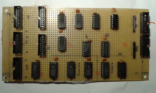
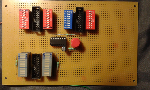
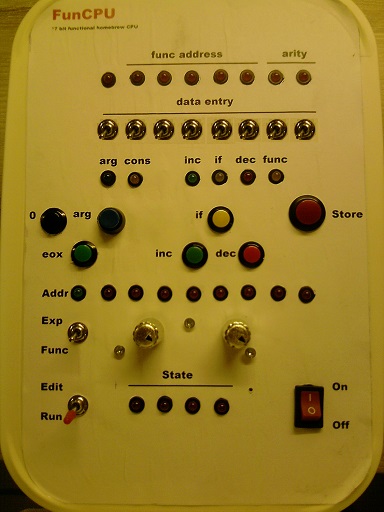
The picture below depicts the overall architecture of the FunCPU. It employs a 8 bit wide databus and a 9 bit wide address bus. Please recall, that although the databus is 8 bits wide, due to the nature of the tagged architecture only 7 out of 8 bits can be used externally (i.e. by the program), and one bit is reserved by the processor to interpret the data. So, from the programmer's point of view the CPU can be considered as a 7-bit CPU, which admittedly is a little odd.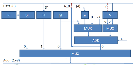
More surprisingly, none of the familiar registers such as PC, SP (stack pointer), accumulator is available. Not even conventional status bits, such as Zero, Overflow flags, etc. can be located (note: although carry bit is present, but it cannot be referenced explicitly or even implicitly by the programmer. More on this later.). This is, because FunCPU employs a rather unconventional, delicate concept for program evaluation.
FunCPU supports 256 bytes of expression memory, in which expressions can be entered and reduced, and also has 256 bytes of function memory, which is dedicated solely to storing user-function definitions. The following internal registers are present:
- RI - reduction index register, is a 8 bit register used for function evaluation.
- DI - is the destination index register. This is a 8 bit register used to access and write destination symbols.
- FI - is the function index register. This is also a 8 bit register, which content is fetched upon entering a function. This register is being incremented as the function definition is being unfolded.
- SI - is the source index register. This is also a 8 bit register pointing to the current symbol of the expression to be reduced.
- ac - is the argument counter. This is a 4 bit register used to support function embedding.
- V - is the value register. This 8 bit register is somewhat analogous to the accumulator utilized in conventional processors, but again its value cannot be read or written by the programmer. V register is used as a termporal storage or a gateway between source and destination expressions.
Please notice that all registers are internal, none of them is exposed to the programmer. The programmer and the user program cannot read, refer to or manipulate these registers explicitly.
The address multiplexer selects among four possible address sources as follows:
- DI is selected (usually) when destination expression is extended/written.
- FI is selected when function definition is accessed.
- SI is selected when source expression is read.
- finally, the ALU output is selected (in a combination when SI and V' are added) to perform argument binding.
The right ALU MUX generates either V or V'. The left ALU MUX either generates a constant of the range from -2 to 1 (also depending on carry bit) or selects SI or ac as one of its inputs.
Please refer to ALU physical implementation for more details.

